*99598*
Isotopetronics:
Fundamentals and Applications.
L.M. Zhuravleva,
Railway University, Obrastzova Street 9,
Moscow 127994, Russia.
V.G. Plekhanov,
Computer Science College, Erika Street 7a,
Tallinn, 10416, Estonia.
Isotopetronics is a new branch of the
nanoscience. The present report is devoted to brief description the
fundamentals and the main applications this new direction: isotope memory
information and solid state processor for quantum computers.
Introduction.
The experience of the past shows that
throughout constant technology improvement electronics (optoelectronics) has
become more reliable, faster, more powerful, and less expensive by reducing the
dimensions of integrated circuits. These advantages are the driver for the
development of modern microelectronics. The long - term goal of this
development will lead to nanoelectronics.
Advancing to the nanoscale is not just a step toward miniaturization, but
requires the introduction and consideration of many additional phenomena. At
the nanoscale, most phenomena and processes are dominated by quantum physics
and they exhibit unique behavior. Nanotechnology includes the integration of
manmade nanostructures into larger material components and systems (see, e.g.
[1]). Importantly, within these larger scale systems, the active elements of
the system will remain at nanoscale.
Low - dimensional structures have become
one of the most active research in nanoscience and nanotechnology.
The seminal works of Esaki and Tsu [2] and
others on the semiconductor superlattice stimulated a vast international
research effort to understand the fabrication and electronic properties of
superlattice, quantum wells, quantum wires and quantum dots (see, for example,
[3 - 6]). The dimensional scale of such samples is between 10 and 100 nm are
subject of nanoscience - is a broad and interdisciplinary field of emerging
research and development. Nanoscience and nanotechnology are concerned with
materials, structures, and systems whose components exhibit novel and
significantly modified physical, chemical properties due to their nanoscale
sizes. New direction of nanoscience is isotopetronics, who is studied the more
low - dimensional size, as a rule the sizes of the sample of isotopetronics
compare to the atomic size. Nuclear technology - neutron irradiation [7] - is
very useful method to preparing low - dimensional structure: quantum wells,
quantum wires and quantum dots [8]. A principal goal of isotopetronics as new directions
of the nanotechnology is to control and exploit their new properties in structures and devices at atomic,
molecular and supramolecular levels. The minituarization required by modern
electronics is one of the driving forces for isotopetronics - new direction of
nanotechnology (see, also [9]).
Results and discussion.
Semiconducting crystals (C, Si, Ge, α - Sn) with diamond - type structure
present ideal objects for studying the isotope effect by the Raman light -
scattering method. At present time this is facilitated by the availability of
high - quality crystals grown from isotopically enriched materials (see, e.g
[10] and references therein). In this part our understanding of first - order
Raman light scattering spectra in isotopically mixed elementary and compound
(CuCl, GaN, GaAs) semiconductors having a zinc blende structure is described.
Isotope effect in light scattering spectra in Ge crystals was first investigated in the paper by
Agekyan et al. [ 11]. A more detailed study
of Raman light scattering spectra in isotopically mixed Ge crystals has been performed by
Cardona and coworkers [10].
It is known that materials having a
diamond structure are characterized by the triply degenerate phonon states in
the Γ point of the
Brillouin zone (k = 0). These phonons are active in the Raman scattering
spectra, but not in the IR absorption
one [28]. Figure 1a demonstrates the dependence of the shape and
position of the first - order line of optical phonons in germanium crystal on
the isotope composition at liquid nitrogen temperature (LNT) [12].
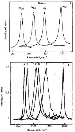 Fig. 1. a - First - order Raman
scattering spectra Ge with different isotope contents [10] and b - First -
order Raman scattering in isotopically mixed diamond crystals ¹²Cx¹³C1-x.
The peaks A, B, C, D, E and F correspond to x = 0.989; 0.90; 0.60; 0.50; 0.30
and 0.001 (after [15]).
Fig. 1. a - First - order Raman
scattering spectra Ge with different isotope contents [10] and b - First -
order Raman scattering in isotopically mixed diamond crystals ¹²Cx¹³C1-x.
The peaks A, B, C, D, E and F correspond to x = 0.989; 0.90; 0.60; 0.50; 0.30
and 0.001 (after [15]).
The coordinate of the center of the
scattering line is proportional to the square root of the reduced mass of the
unit cell, i.e. √M. It is precisely this dependence that is expected in
the harmonic approximation. An additional frequency shift of the line is
observed for the natural and enriched germanium specimens and is equal, as
shown in Ref. [10] to 0.34 ± 0.04 and 1.06 ± 0.04 cm⁻¹, respectively
(see, e.g. Fig. 7 in Ch. 4 of Ref. [14]).
First - order Raman light - scattering
spectrum in diamond crystals also includes one line with maximum at ωLTO(Γ) = 1332.5 cm⁻¹. In Fig. 1b
the first - order scattering spectrum in diamond crystals with different
isotope concentration is shown [15]. As shown below, the maximum and the width
of the first - order scattering line in isotopically - mixed diamond crystals
are nonlinearly dependent on the concentration of isotopes x. The maximum shift
of this line is 52.3 cm⁻¹, corresponding to the two limiting values
of x = 0 and x = 1. Analogous structures of first - order light scattering
spectra and their dependence on isotope composition has by now been observed
many times, not only in elementary Si, and α - Sn, but also in compound CuCl and GaN
semiconductors (for more details see reviews [10, 16]). Already short list of
data shows a large dependence of the structure of first - order light -
scattering spectra in diamond as compared to other crystals (Si, Ge). This is
the subject detailed discussion in [17]. Second - order Raman spectra in
natural and isotopically mixed diamond
and LiH - LiD have been studied and rather detailed described in reviews
(see, e.g. [17]).
Isotopic substitution only affects the
wavefunction of phonons; therefore, the energy values of electron levels in the
Schrödinger equation ought to have remained the same. This, however, is
not so, since isotopic substitution modifies not only the phonon spectrum, but
also the constant of electron-phonon interaction (see, e.g. [16]). It is for
this reason that the energy values of purely electron transition in molecules
of hydride and deuteride are found to be different ([16] and references
therein). This effect is even more prominent when we are dealing with a solid
[18]. Intercomparison of absorption spectra for thin films of LiH and LiD at room
temperature revealed that the longwave maximum (as we know now, the exciton
peak [16]) moves 64.5 meV towards the shorter wavelengths when H is replaced
with D. For obvious reasons this fundamental result could not then receive
consistent and comprehensive interpretation, which does not be little its
importance even today. As will be shown below, this effect becomes even more
pronounced at low temperatures (see, also [17]).
The mirror reflection spectra of mixed and
pure LiD crystals cleaved in liquid helium are presented in Fig. 2.
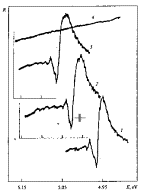
Fig. 2. Mirror reflection spectra of
crystals: 1 - LiH; 2 - LiHxD 1-x; 3 - LiD; at 4.2 K. 4 -
source of light without crystal. Spectral resolution of the instrument is
indicated on the diagram (after [7]).
For comparison, on the same diagram we
have also plotted the reflection spectrum of LiH crystals with clean surface.
All spectra have been measured with the same apparatus under the same conditions.
As the deuterium concentration increases, the long-wave maximum broadens and
shifts towards the shorter wavelengths. As can clearly be seen in Fig. 6, all
spectra exhibit a similar long-wave structure. This circumstance allows us to
attribute this structure to the excitation of the ground (Is) and the first
excited (2s) exciton states. The energy values of exciton maxima for pure and
mixed crystals at 2 K are presented in Table 17 of Ref. [19]. The binding
energies of excitons Eb, calculated by the hydrogen-like formula,
and the energies of interband transitions Eg are also given in Table
17 of ref. [19]. Going back to Fig.
2, it is hard to miss the growth of Δ₁₂, [18], which in the
hydrogen-like model causes an increase of the exciton Rydberg with the
replacement of isotopes (see Fig. 90 in [16]). When hydrogen is completely
replaced with deuterium, the exciton Rydberg (in the Wannier-Mott model)
increases by 20% from 40 to 50 meV, whereas Eg exhibits a 2%
increase, and at 2 ÷ 4.2 K is ΔEg = 103 meV. This quantity depends
on the temperature, and at room temperature is 73 meV, which agrees well enough
with ΔEg
= 64.5 meV as found in early the paper of Kapustinsky et al. [20]. Isotopic substitution of the light
isotope (³²S) by the heavy one (³⁴S) in CdS crystals [19]
reduces the exciton Rydberg, which was then attributed to the tentative
contribution from the adjacent electron bands (see also [19), which, however,
are not present in LiH (for the details see e.g. reviews [14, 10, 16]).
Further we briefly
discuss the density of optical states in different size - structures: one - ,
two and three - dimension (see, also [22]). Traditionally, microelectronics is
based on scaling towards smaller structures. When the dimension of these structures reach the nanometric scale,
microelectronics has already transformed to nanoelectronics. As was mentioned
above, new directions of nanoscience is isotopetronics, who is studied the more
low - dimensional size, as a rule the sizes of the sample of isotopetronics compare
to the atomic size. The band diagram of a material depends on its crystal
structure and on the material wavefunction of the electrons (see, e.g.
[22]). The band diagram reveals the
energy level that can be occupied.. The density of states (DOS) of these levels
depend on the size of the crystal. An extensive three - dimensional body
produces a three - dimensional k - space. The energy E of the electrons can be
derived from solid - state physics as [22]:
E = ((ℏ²)/(2m))(kx² + ky² + kz²)
= ((ℏ²)/(2m))∣k∣². (1)
With respect to the three - dimensional k
- space the possible states can be expressed as:
S = ((VT)/(3π²))(((2mE)/(ℏ²)))3/2. (2)
The DOS follows as:
((dS)/(dE)) = √2((VTm3/2)/(π²ℏ²))√E. (3)
The DOS is proportional to the square root
of the energy of the electrons. This function describes the well - known
Bolzman relation of classical physics (see, also Fig. 3). A three - dimensional relatively large
ashlars (3D potential well) has a steady √E characteristic for the DOS,
whereas the DOS characteristics becomes discontinuous if at least a single
dimension is scaled down to the domain of the material wavelength of an
electron. This leads to quantum layers (2D potential well) and appears, e.g. in
the inversion layer of a metal - oxide - semiconductor transistor [22]. Further
steps lead to the quantum wire (1D potential well and a quantum dot (0D
potential well). an electron space that is limited in one direction leaves an
unlimited two - dimensional k - space for the electron. In this case of a
quantum layer the energy of the particle is:
E = ((ℏ²)/(2m))(kx² + ky²) + Ei.
(4)
Along the reduced dimension only states
that match with the wavelength of the electrons can appear. Therefore, dicrete
energy levels Ei appear.
Because of the two - dimensional k - space the DOS S is directly proportional
to E. If this expression is derived to E, dS/dE is independent of the energy (see, Fig. 3).
A further step leads to the so - called
quantum wire, which leaves only one
dimension of freedom to the electron. Consequently, the energy can be expressed
as:
E = ((ℏ²)/(2m))(kx² ) + Ein.
(5)
Under this condition the DOS is for one -
dimensional k - space inversely proportional to the square root of the energy.
A restriction of all three dimensions of the DOS only discrete lines can
appear,
E = Eimn.
(6)
In this case the DOS shows only discrete
lines, similar to a hydrogen atom or a molecule (see, Fig. 3). Such a quantum
dot can be realized from a small semiconductors columns.
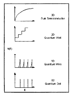
Fig. 3. Density of electronic states as a
function of structure size.
In general, the lateral dimensions are
adjusted so that the energy value of an electron is about one eV. The third
dimension depends on a very thin epitaxial layer [22]. With respect to this
dimension the electrons own at least twenty eV. This result in a clearly arranged energy spectrum since vertical
energy levels only appear at higher energy levels. This arrays can be tuned to desired wavelengths and emit sufficient power for laser applications
(see, also below). Detailed description of the low - dimensional structures of
isotope - mixed crystals can be found in Refs. [22 - 23].
The knowledge gained in above discussion
makes it possible to consider and analyze a variety of different nanostructure
devices. In this part we consider electronic and optical devices. Some of these mimic well - known
microelectronic devices but with small dimensional scales. This approach
applications to devices with shorter response times and higher operational
frequencies that operate at lower
working currents, dissipate less power, and exhibit other useful properties and enhanced characteristics. Such example
include, in the first step, the field effect transistors will be consider
below. On the other hand, new generations of the devices are based on new
physical principles, which can not realized in microscale devices. Among these
novel devices are the resonant - tunneling devices described in next
section, and single - electron -
transistor as well as optoelectronic devices (light - emitting diodes and
lasers).
As is well - known the diodes are simplest
electronic devices, for which the current is controlled by the diode bias and
vice versa. A useful function can be performed mainly due to nonlinearity of
current - voltage dependences. In contrast, in three - terminal devices known
as transistors there exist the
possibility of controlling the current
through two electrodes by varying the voltage or the current through third
electrode. Below we briefly describe
the field effect transistors (FETs) on
the base of the nanowires. Nanowire FETs can be configurated by depositing the
nanomaterial onto an insulating substrate surface, and making source and drain
on the ends nanowire. Fig. 4 illustrates this approach. There , we show a
schematic diagram of a Si - nanowire
FET with the nanowire, the metal source and drain electrodes on the surface of
the SiO₂/Si substrate (see, also [22]).
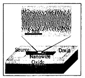
Fig. 4. A schematic diagram of a Si - FET
with nanowire, the metal source, and drain electrodes on the surface of a SiO₂/
Si substrate (after [25]).
This approach may serve as the basis for hybrid electronic
systems consisting of nanoscale
building blocks integrated with more complex planar silicon circuitry [6]. We
should note that an extremely small FET may be built on the basis of carbon
nanotube. In conclusion of this part we have noted that the nanowire devices
discussed here have great potential for applications in nano - and
optoelectronics.
The so - called single electronics [22 - 26] appeared in the late 1980s, is
at present time a tremendously expanded research field covering future digital and analog circuits, metrological
standards, sensors, and quantum information processing and transfer [6]. The basic device, called a single electron
device (SED), literally enables the control of electrons on the level of an
elementary charge. There are rich varieties SEDs (see, e.g. [22] and references
therein), but the operation principle
of all SED is basically the same (see, Fig. 5).
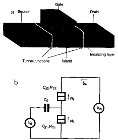 Fig. 5. The single electron tunneling transistor (SET). a -
Simplified three - dimensional structure of the SET. The channel of the FET is
replaced here by a sandwich consisting of a nanoscal metal electrode (island),
which is connected to the drain and the source by tunnel junctions. AS in FET,
a gate electrode influences the island electrostatically. b - Circuit diagram of the SET. The square box
symbol represents a tunnel junction,
and integers N₁ and N₂ denote the numbers of electrons having
through the two junctions Each junctions is characterized by its capacitance
and its tunnel resistance (after [24]).
Fig. 5. The single electron tunneling transistor (SET). a -
Simplified three - dimensional structure of the SET. The channel of the FET is
replaced here by a sandwich consisting of a nanoscal metal electrode (island),
which is connected to the drain and the source by tunnel junctions. AS in FET,
a gate electrode influences the island electrostatically. b - Circuit diagram of the SET. The square box
symbol represents a tunnel junction,
and integers N₁ and N₂ denote the numbers of electrons having
through the two junctions Each junctions is characterized by its capacitance
and its tunnel resistance (after [24]).
SEDs rely on a phenomenon that occurs when
electrons are to enter a tiny conducting material. When the tiny conducting
material, or metallic "island", is extremely small, the electrostatic
potential of the island significantly
increases even when only one electron enters it. For example, for a nanometer
scale island having a capacitance C of, say, 1 aF (10⁻¹⁸F),
the increase in the voltage, which is e/C with e = 1.6 ⋅ 10⁻¹⁹ C, reaches 16 mV. This is much larger than the
thermal noise voltage at room temperature, 25.9 mV. Coulomb repulsion prevents
additional electrons from entering the island unless the island potential is
intentional lowered by an external bias. If the island potential is lowered
gradually, the other electrons can enter the island one by one with negligibly
small power dissipation .
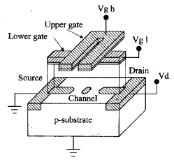 Fig. 6. Single - electron transistor on the base of the MOP
with double block (after [22]).
Fig. 6. Single - electron transistor on the base of the MOP
with double block (after [22]).
The single - electron transistor works as
follows (Figs. 6 - 7). The electron transfer is determined by two factors: the
Coulomb charging of the dot and the quantized energy levels in the dot (see
above).
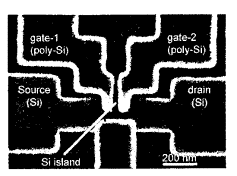
Fig. 7. A scanning electron microscope
image of a single electron transistor (after [25]).
If the drain is biased with respect to the
source, an electric current occurs in the regime of single - electron transfer. By applying the voltage
to the gate and changing the QD
parameters, one can change the conditions of electron tunneling and affect the
source - drain current. Examples of
modulation of the conductance in single - electron transistors by the gate voltage are presented in Fig. 8.
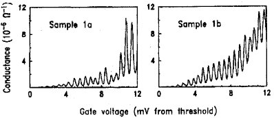
Fig. 8. Conductance as a function of Vg
for two samples with the same geometry (after [26]).
The devices have almost the same geometry.
Their dimensions are large enough to have a number of quantized levels. In Fig.
8 each peak in the conductance corresponds to transfer of one electron, when an
energy level enters into resonance with the electron states in the contacts.
Though the conductance versus gate - voltage dependences are different, i.e.
not reproducible, the peak spacing is the same for both devices. It is
determined by the change in the gate
voltage required to change the charging
energy of the QDs by one electron. The Fig. 8 shows clearly that the electric
current is modulated significantly by the gate voltage. Thus, for transistors
with single - electron transport, strong control of very small electric current
may be possible.
So far we have studied electronic
nanoscale devices, i.e., a class of devices that exploits electrical properties
of nanostructures and operates with electric input and output signals.
another class is composed of optoelectronic devices, which are based on
both electrical and optical properties of materials and work with optical and
electric signals. In this paragraph we
will analyze two very important classes of optoelectronic devices: light -
emitting diodes and lasers (diodes as well as photodetectors. As will be shown
below, the energy of the electric current flowing through these diodes is
transformed into light energy. These optoelectronic devices have a huge number
of applications and deserve consideration in details (see, also [22 - 31]).
Although stimulated emission [14] from the
injection laser diode is very important (see, below), practically, sub -
threshold operation of the diode - when only spontaneous light is emitted - is
in many cases advantageous and has a number of applications. Diodes operating with spontaneous light
emission are called light - emitting diodes [31]. The important characteristic
of the light - emitting diode is the spectral distribution of emission The
spectrum of emission is determined,
primarily, by the electron/hole distributions. Thus, the ambient temperature T,
defines both spectral maximum and the spectral width of emission. The peak
value of the spectral distribution can be estimated as [3]
ℏω = Eg + ((kBT)/2). (7)
The full width at half maximum of the distribution is Δω ≈ 2kBT/ℏ and is independent of ω. In terms of the wavelength, λ, we obtain
Δλ = [λm²/(2πc)Δω
or
Δλ = 1.45λ²kBT, (8)
where λ_{m}
corresponds to the maximum of the spectral distribution, Δλ and λ_{m}
are expressed in micrometers, and kBT is expressed in eV. Fig. 41 in [22] shows
the spectral density as a function of the wavelength for light - emitting
diodes based on various materials. For
these different materials, the spectral linewidth increase in proportion to λ², in accordance with Eq. (8).
From indicated figure, one can see that light - emitting diodes cover a wide
spectral region from the infrared - about 8 μm for InGaAsP alloys - to the near ultraviolet
- 0.4 μm for GaN.
Light - emitting diodes are, indeed very universal light sources [9].
Semiconductor lasers incorporating low -
dimensional hetero-structures., QWs and QDs, are attracting considerable
interest of their potential for improved performance over QW lasers (see, e.g.
[31]). This prediction is based, in the single - particle picture, on the
sharper density of states resulting from the confinement of the charge carriers
in two or three directions. Among other advantages, the ideal QD and QWr lasers
would exhibit higher and narrower gain spectrum, low threshold currents, better
stability with temperature, lower diffusion of carriers to the device surfaces,
and a narrower emission line than double heterostructure or QW lasers (see,
also [22]). The observation of lasing
from excitons in optically excited V - groove GaAs/AlGaAs QWr laser structures
was detail describe in paper [27]. The observable emission is attributed to the
recombinations of excitons associated with the lowest energy electron - and
hole - subbbands of the QWr. Moreover these authors show that the emission
energy remains nearly constant within the inhomogeneously broadened
photoluminescence line of the QWrs for both continuous wave and pulsed optical
excitation over a wide range of power densities. These results corroborate the
important role played by electron - hole Coulomb correlations in the optical
emission from quasi - 1D QWrs in the density regime of the Mott transition.
Optical emission of the QWr laser
structure are displayed in Fig. 9 for different values of the optical power
density below, at and above the threshold for lasing in the QWr.
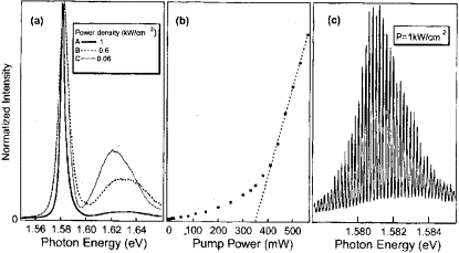
Fig. 9. (a) Photoluminescence spectra at
10 K of the QWr laser sample above, below and near the lasing threshold in TE -
polarization. (b) Dependence on input excitation power of the PL output
power;arrows indicate the excitation powers used for the optical spectra
depicted in (a). (c) High resolution emission spectrum above the lasing
threshold showing the Fabri - Perrot modes of the optical cavity (after [27]).
Upon increasing the pump power, these
authors observe a nearly constant energy of the peak at 1.581 eV that
corresponds to the optical transition e₁ - h₁ associated with the
ground electron - hole - subband of the QWrs. A significant spectral narrowing
is also found as the power density is increased and crosses the lasing
threshold. This evidences the existence of amplified spontaneous emission
within this inhomogeneously broadened PL line in this density regime. The observable emission intensity varies linearly
at low excitation power over three orders
of magnitude (from 0.1 to 100 mW) [27]). Above the lasing threshold (at
350 mW) the intensity variation is again linear (see, Fig.9^{b}), indicating
that the modal gain is saturated. In Fig. 9^{c}, a high - resolution emission
spectrum obtained above threshold features well - resolved Fabry - Perot modes
that correspond to different longitudinal optical modes within the
inhomogeneuous line of the QWr - PL (see also Fig. 10). Detailed investigations
of PL and PLE spectra (see, Fig. 43 in [22]) of the QWr allowed the indicated
authors to conclude that the lasing emission originates from the recombination
of excitons as it is case for the QWr - peak of the cw - PL spectrum (details
see [27]).
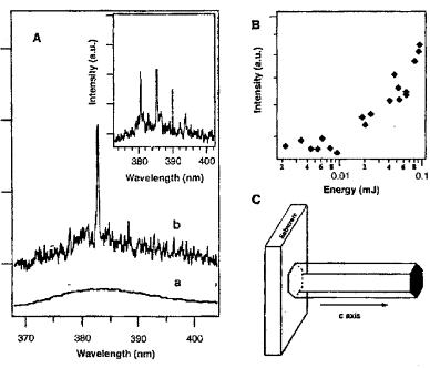
Fig. 10. (A) Emission spectra from
nanowire arrays below (line a) and above (line b and inset) the lasing
threshold. The pump power for these spectra are 20, 100 and 150 kW/cm²,
respectively. The spectra are offset for easy comparison. (B) Integrated
emission intensity from nanowires as a function of optical pumping intensity.
(C) Schematic illustration of a nanowire as a resonance cavity with two
naturally faceted hexagonalend faces acting as reflecting mirror. Stimulated
emission from the nanowires was
collected in the direction along the nanowire's end - plane normal (the
symmetric axis) with a monochromator
combined with a Peltier - cooled charge - coupled device. The 226 - nm
pump beam was focused to the nanowire array at an angle 10⁰ to the end -
plane normal.All experiments were carried at room temperature (after [30]).
In QDs, as indicated above, carriers are
confined in the three directions in a very small region of space, producing quantum effects in the
electronic properties. As we can see
from Fig. 3, the electronic joint density of states for QD shows sharp peaks
corresponding to transitions between discrete energy levels of electrons and
holes. Outside these levels the DOS vanishes. In many ways, the electronic
structure of a QD resembles that a single atom. Lasers based on QDs could
have properties similar to those of
conventional ion gas lasers, with the advantage that the electronic structure
of a QD can be engineered by changing the base material, size and shape. In the
next we assume that the QDs are small enough
so that the separation between the first two electron energy levels for
both electrons and holes is much larger than the thermal energy kT. Then for an
undoped system, injected electrons and holes will occupy only the lowest level.
Therefore, all injected electrons will contribute to the lasing transitions
from the E1e to the E1hh levels, reducing the threshold
current with respect to other systems with lower confinement. The evolution of
the threshold current density obtained along the years for various laser structures is shown in
Fig.11.
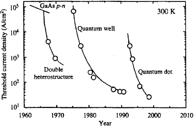
Fig.11. Evolution of threshold current
density for lasers based on different confinement structures (after [29]).
The lowest threshold currents have already
been reached for QD lasers [22]. As long as the thermal energy is lower than
the separation between the fist and second
levels, the emission band in an ideal QD laser is very sharp and does not
depend on temperature (see, also [31].
Therefore, QD lasers should have a better stability with temperature
without the need for cooling. We should
add that QDs have the narrowest spectrum
and the highest gain.
References.
1. K. Goser, P. Glösekötter, J.
Dienstuhl, Nanoelectronics and Nanosystems (Berlin, Springer, 2004).
2. L. Esaki and R. Tsu, Supelattice and
negative differential conductivity in semiconductors, IBM J. Res. and Develop. 14, 61 (1970).
3. M.J. Kelly, Low - dimensional Semiconductors (Oxford, Clarendon Press, 1995).
4. J.H. Davis, The Physics of Low -
dimensional Semiconductors (Cambridge, Cambridge University Press, 1998).
5. P. Harrison, Qquantum Wells, Wires and
Dots (New York, Wiley, 2001).
6. L. Esaki, in Molecular Beam Epitaxy and
Heterostructures, ed. by L.L. Chang, K. Ploog (Dordrecht, Kluwer Academic,
1985).
7. V.G. Plekhanov, Applications of the
Isotopic Effect in Solids (Berlin - Heidelberg, Springer, 2004).
8. V.G. Plekhanov, Isotope - based quantum
information, ArXiv: quant - ph/ 0909.0820 (2009).
9. Single Semiconductor Quantum Dots, P.
Michler (ed.) (Berlin - Heidelberg, Springer - Verlag, 2009).
10. M. Cardona and M.L.W. Thewalt, Isotope
effect on optical spectra of semiconductor, Rev. Mod. Phys. 77, p. 1173
- 1224, October 2005.
11. V.F. Agekyan, A.M. Asnin, V.M. Kryukov
et al., Isotope effect in germanium, Fiz. Tverd. Tela 31, (No 12) p. 101
-104 (1989) (in Russian).
12. M. Lax, E. Burstein, Infrared lattice
absorption in ionic and homopolar crystals, Phys. Rev. 97 (No 1) p. 39 - 52 (1955).
13. H.D. Fuchs, P. Etchegoin, M. Cardona
et al., Vibrational band modes in
germanium: Isotopic disorder - induced Raman scattering, Phys. Rev. Lett 70,
p. 1715 - 1718 (1993).
14. V.G. Plekhanov, Isotope Effect in
Solid State Physics, in Semiconductors and Semimetals, Vol. 68 (R.K. Willardson
and E. Weber (eds.)) (San Diego, CA, Academic Press, 2001).
15. H.Hanzawa, N. Umemura, Y. Nishida and
H. Kanda, Disorder effect of nitrogen impurities, irradiation - induced defects
and ¹³C composition on the Raman spectrum in syntethic I^{b} diamond,
Phys. Rev. B54 (No 6) p. 3793 - 3799 (1996).
16. V.G. Plekhanov, Elementary excitations
in isotope - mixed crystals, Phys. Rep. 410 (No 1 - 3) p. 1 - 235
(2005).
17. V.G. Plekhanov, Isotope effects in
lattice dynamics, Physics - Uspekhi 46 (No 7) p. 689 - 715 (2003).
18. V.G. Plekhanov, Experimental evidence
of strong phonon scattering in isotopical disordered systems: the case LiHxD
1-x, Phys. Rev. B51 (No ) p. 8874 - 8878 (1995); ArXiv: cond
- mat/ 0907.3817.
19. V.G. Plekhanov, Manifestation and
Origin of the Isotope Effect, ArXiv:phys/ 0907.2024 (2009).
20. A.F. Kapustinsky, L.M. Shamovsky, K.S.
Bayushkina, Thermochemistry of isotopes, Acta physicochem (USSR) 7 (No
6) p. 799 - 810 (1937).
21. F.I. Kreingol'd, K.F. Lider, M.B.
Shabaeva, Influence of isotope substitution sulfur on the exciton spectrum in
CdS crystal, Fiz. Tverd. Tela 26 (No 11) p. 3940 - 3941 (1984) (in
Russian).
22. V.G. Plekhanov, Isotopetronics - new
direction of nanoscience, ArXiv:phys/1007.5386 (2010).
23. L.M. Zhuravleva, V.G. Plekhanov,
Nuclear technology in creation of low - dimensional isotope - mixed structures,
Nanoindustry 4, (N 16) 32 - 35 (2009); Isotopical nanotechnology low -
dimensional structures, Nano - and Microsystematic Technique N9 (122) 8
- 12 (2010) (in Russian).
24. M.H. Devoret and R.J. Schoelkopf,
Amplifying quantum signals with the single - electron transistors, Nature 406,
1039 - 1046 (2000); Y. Ono, A. Fujiwara, K. Nishiguch, et al., Manipulation and
detection of single electrons for future information processing, J. Appl. Phys.
97 (N 3) p. 031101 - 19 (2005).
25. Y. Ono and Y. Takahashi, Electron pump
by a combined single - electron field - effect transistor, Appl. Phys. Lett. 82, 1221 1223 (2003).
26. M.A. Kastner, The single electron
transistor, Rev. Mod. Phys. 64, 849 - 858 (1992).
27. L. Sirigu, D.Y. Oberli, L. Deriorgi et
al., Excitonic lasing in semiconductor quantum wires, Phys. Rev. B61 (N
10) p. R10575 - 4 (2000).
28. L.A. Colderen and S.W. Corzine,
Diode Lasers and Photonic Integrated Cicuits (New York, Wiley, 1995).
29. L.M. Zhuravleva and V.G. Plekhanov (in
press).
30. M.H. Huang, S. Mao, H. Feick et al.,
Room - temperature ultraviolet nanowire nanolasers, Science 292, 1897 - 1899 (200).
31. V.M. Ustinov, A.E. Zukov, A.Yu. Egorov
ans N.A. Maleen, Quantum Dot Lasers (Oxford, Oxford University Press, 2003).